Journal Articles
[56] C. S. Prasad, H. O. Everitt, and G. V. Naik, “Thermal imaging through hot emissive windows,” (under review).
[55] Z. Li, C. S. Prasad, X. Wang, D. Zhang, and G. V. Naik, “Sensing beyond the exceptional point for high detectivity,” (under review).
[54] B. B. Jerome*, C. S. Prasad*, A. Schirato*, O. S. Dewey, J. Doumani, A. Baydin, W. Gao, G. Della Valle, J. Kono, M. Pasquali, G. V. Naik, and A. Alabastri, “Coupling into Hyperbolic Carbon-Nanotube Films with a Deep-Etched Antenna Grating,” ACS Photonics, (2023). [pdf] (*equal contribution)
[53] Z. Li, C. S Prasad, X. Wang, D. Zhang, R. Lach, G. V Naik, “Balancing detectivity and sensitivity of plasmonic sensors with surface lattice resonance,” Nanophotonics, vol. 12, no. 19, pp. 3721-3727 (2023). [pdf]
[52] Y. Chong, H. O. Everitt, V. Galdi, M. Khajavikhan, and G. V. Naik, “Non-Hermitian optics and photonics: introduction to the special issue,” Optical Material Express, vol. 13, no. 6, pp. 1710-1711 (2023). [pdf]
[51] M. Izadparast, G. V. Naik, H. O. Everitt, and H. Ramezani, “Exceptional point based lattice gyroscopes,” Optical Material Express, vol. 13, no. 6, pp. 1547-1554 (2023). [Feature issue on Non-Hermitian Optics & Photonics] [pdf]
[50] C. F. Doiron, J. B. Khurgin, and G. V. Naik, “Super-Mossian dielectrics for nanophotonics,” Advanced Optical Materials, vol. 10, no. 22, p. 2201084 (2022). [pdf]
The refractive indices of dielectrics cannot be arbitrarily high and follow a trend given by Moss’s rule. However, some materials surpass the Moss rule and are super-Mossian dielectrics. This paper sheds light on why some materials are super-Mossian. This work shows that iron pyrite is a better dielectric than silicon in near-infrared and surpasses Moss’s rule by 39%.
[49] W. Li, Y. He, K. Yang, and G. V. Naik, “Scaling electrical percolation networks based on renormalization group theory,” Applied Physics A, vol. 128, p. 685 (2022). [pdf]
Can the statistical data of a small area of a percolation network predict the statistical data of a larger area? Here, an algorithm is provided to accomplish it. A small-area SEM image of an ultra-thin metal film is sufficient to know the mean and variance of resistance distribution across any region of this film.
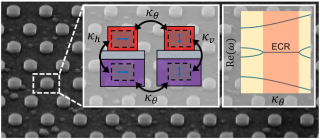
[48] F. Yang, C. S. Prasad, W. Li, R. Lach, H. O. Everitt, and G. V. Naik, “Non-Hermitian metasurface with non-trivial topology,” Nanophotonics, vol. 11, no. 6, pp.1159-1165 (2022). [pdf]
Topology is often synonymous with edge states. However, bulk states can possess a non-trivial topology. Here, we demonstrate an exceptional concentric ring (ECR) possessing Z3 topology in a non-Hermitian metasurface.
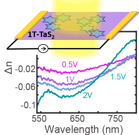
[47] W. Li, and G. V. Naik, “Reorganization of CDW stacking in 1T-TaS2 by an in-plane electrical bias,” APL Materials, vol. 9, p. 111103, 2021. (Invited to the special issue on Light and Matter Interactions) [pdf]
An in-plane electrical bias tunes the optical constants of 1T-TaS2. We find out that electrical bias forces the CDW domains towards ground state stacking and thereby resulting in a huge optical tunability.
[46] F. Yang, A. Hwang, C. F. Doiron, and G. V. Naik, “Non-Hermitian metasurfaces for the best of plasmonics and dielectrics,” Optical Materials Express, vol. 11, no. 7, pp. 2326-2334, 2021. (Editor’s pick) [pdf]
We demonstrate that non-Hermitian physics allows turning undesirable optical loss into a useful design parameter. Here, we elucidate the design principles for nanophotonic passive PT-symmetric systems.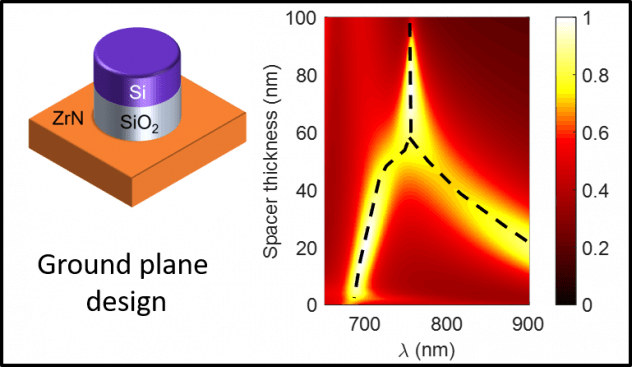
[45] W.Li, and G. V. Naik, “Light-induced reorganization of charge density wave stacking in 1T-TaS2,” Applied Physics Letters, vol. 118, p. 253104, 2021. (Invited to the special issue on charge density waves) [pdf]
Temperature is an important tool in understanding light-induced reorganization of CDW stacking in 1T-TaS2. Here, we find out that illumination causes the boundaries between differently stacked domains to move and favor one stacking more over the other.
![]()

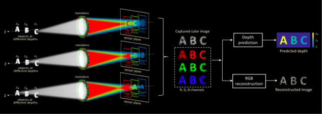
[44] S. Tan, F. Yang, V. Boominathan, A. Veeraraghavan, G. V. Naik, “3D Imaging Using Extreme Dispersion in Optical Metasurfaces,” ACS Photonics, vol. 8, no. 5, pp. 1421–1429, 2021. [pdf]
Exploiting the huge chromatic dispersion of metasurfaces, we propose an all-color, wide field-of-view (FOV), metalens camera that uses computational imaging to accurately extract the depth information in a single shot.
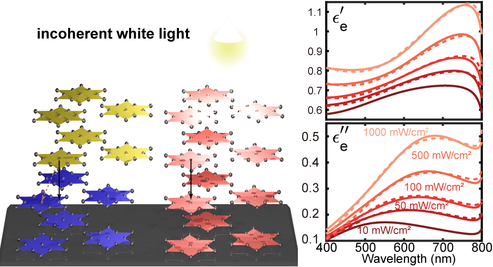
[43] W. Li, and G. V. Naik, “Large Optical Tunability from Charge Density Waves in 1T-TaS2 under Incoherent Illumination,” Nano Letters, vol. 20, no. 11, pp. 7868-7873, 2020. (Cover picture) [pdf]
Tunable optical materials are necessary for many emerging nanophotonic applications. Here we report a new class of tunable optical material, 1T-TaS2, a quantum material exhibiting unity order index change under low-intensity (~1 sun) incoherent illumination.
[42]
Though theoretical estimates predict 80% conversion efficiency for the thermophotovoltaic scheme, the current efficiency record is less than 20%. Here we investigate the spectral selectivity of the thermal emitter for improving efficiency. 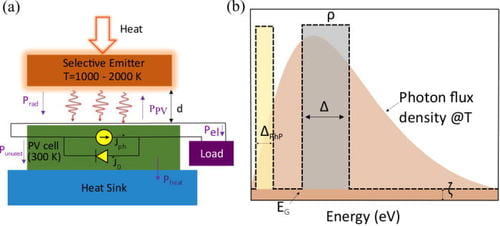
[41] W. Gao, N. Komatsu, L. Taylor, G. V. Naik, K. Yanagi, M. Pasquali, and J. Kono, “Macroscopically aligned carbon nanotubes for flexible and high-temperature electronics, optoelectronics, and thermoelectrics,” Journal of Applied Physics: D, vol. 53, no. 6, p. 063001, 2019. [pdf]
A review of recent developments in the electronic, optical, optoelectronic, and thermoelectric applications of wafer-scale aligned carbon nanotubes is presented here.
[40] C. F. Doiron, and G. V. Naik, “Non‐Hermitian selective thermal emitters using metal-semiconductor hybrid resonators,” Advanced Materials, vol. 31, p. 19041542019, 2019 [pdf]
A quantum optical description of thermal light sources leads to an interesting paradigm with many new design tools. This paper is the first demonstration of thermal emitters designed using quantum physics of open systems.
[39] W. Gao*, C. F. Doiron*, X. Li, J. Kono, and G. V. Naik, “Macroscopically aligned carbon nanotubes as a refractory platform for hyperbolic thermal emitters,” ACS Photonics, vol. 6, no. 7, pp. 1602-1609, 2019. [pdf]
Nanophotonics at high temperatures (> 500 deg C) is limited by the lack of good refractory optical materials. Here, we demonstrate that wafer-scale aligned carbon nanotubes (CNTs) make an excellent refractory nanophotonic material platform.

[38] W. Li and G. V. Naik, “In-plane electrical bias tunable optical properties of 1T-TaS₂,” Optical Material Express, vol. 9, no. 2, pp. 497-503, 2019. [Invited to Special Issue on Photonics with Ultra-thin and Atomically-thin Materials] [pdf]
Tunable optical materials make the core of tunable nanophotonic devices. Tunability of such materials is either too slow or too small. Here, we report a new class of materials exhibiting charge density waves (CDW) with moderately fast and large tunability.
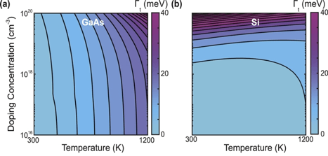
[37] C. F. Doiron and G. V. Naik, “Semiconductors for high selectivity thermal emitters,” Journal of Optics, vol. 20, no. 8, p. 084001, 2018. [Invited to Special Issue on New Materials for Nanophotonics] [pdf]
Semiconductors are promising for high temperature [600-1200 K] nanophotonics owing to their small optical losses, tunable optical properties, and well-established nanofabrication methods. However, their high-temperature optical properties are unknown and difficult to predict. Here we present a semi-empirical method to predict the optical properties of common semiconductors in a wide range of doping and temperatures.
[36] T. Tumkur, X. Yang, C. Zhang, J. Yang, Y. Zhang, G. V. Naik, P. Nordlander, and N. J. Halas, “Wavelength-Dependent Optical Force Imaging of Bimetallic Al–Au Heterodimers,” Nano Letters, vol. 18, no. 3, pp. 2040–2046, 2018. [pdf]
Near-field imaging of forced plasmons in bimetallic heterodimers using Photo-induced Force Microscopy (PIFM) at different excitation wavelengths in visible shows how strong plasmonic resonance in a gold nanoparticle excites otherwise weak plasmons in a coupled aluminum nanoparticle.

*** *** ***
[35] M. Parente, S. Sheikholeslami, G. V. Naik, J. A. Dionne, and A. Baldi, “Equilibration of Photogenerated Charge Carriers in Plasmonic Core@Shell Nanoparticles,” Journal of Physical Chemistry C, vol. 122, no. 41, pp. 23631–23638, 2018. [pdf]
[34] D. M. Wu, M. L. Solomon, G. V. Naik, A. García-Etxarri, M. Lawrence, A. Salleo, and J. A. Dionne, “Chemically Responsive Elastomers Exhibiting Unity-Order Refractive Index Modulation,” Advanced Materials, vol. 30, no. 7, p. 1703912, 2018. [pdf]
[33] G. V. Naik, A. J. Welch, J. A. Briggs, M. L. Solomon, and J. A. Dionne, “Hot-Carrier-Mediated Photon Upconversion in Metal-Decorated Quantum Wells,” Nano Letters, vol. 17, no. 8, pp 4583–4587, 2017. [pdf]
[32] J. A. Briggs, G. V. Naik, , “Temperature-dependent optical properties of titanium nitride,” Applied Physics Letters, vol. 110, p. 101901, 2017. [pdf]
[31] J. A. Briggs, G. V. Naik, T. A. Petach, B. K. Baum, D. Goldhaber-Gordon and J. A. Dionne, “Fully CMOS-compatible titanium nitride nanoantennas,” Applied Physics Letters, vol. 108, p. 051110, 2016. [pdf]
[30] J. Kim, A. Dutta, G. V. Naik, A. V. Kildishev, A. J. Giles, F. J. Bezares, C. T. Ellis, J. G. Tischler, O. J. Glembocki, A. M. Mahmoud, H. Caglayan, J. D. Caldwell, A. Boltasseva, and N. Engheta, “The Role of Epsilon-Near-Zero Substrates in the Optical Response of Plasmonic Antennas,” Optica, vol. 3, no. 3, pp. 339-346, 2016. [pdf]
[29] J. A. Dionne, A. Baldi, B. Baum, C-S. Ho, V. Jankovic, G. V. Naik, T. Narayan, J. A. Scholl, and Y. Zhao, “Localized fields, global impact: Industrial applications of resonant plasmonic materials,” MRS Bulletin, vol. 40, no. 12, pp. 1138-1145, 2015. [pdf]
[28] G. V. Naik, and J. A. Dionne, “Photon upconversion with hot carriers in plasmonic systems,” Applied Physics Letters, vol. 107, p. 133902, 2015. [pdf]
[27] T. Wang, M. Zalkovskij, K. Iwaszczuk, A. V. Lavrinenko, G. V. Naik, J. Kim, A. Boltasseva, and P. U. Jepsen, “Ultrabroadband terahertz conductivity of highly doped ZnO and ITO,” Optical Materials Express, vol. 5, no. 3, pp. 566-575, 2015. [pdf]
[26] B. Saha, S. Saber, G. V. Naik, A. Boltasseva, E. A. Stach, E. P. Kvam, and T. D. Sands, “Development of epitaxial AlxSc1-xN for artificially structured metal/semiconductor superlattice metamaterials,” Physica Status Solidi B, vol. 252, no. 2, pp. 251-259, 2015. (Editor’s choice and Cover picture) [pdf]
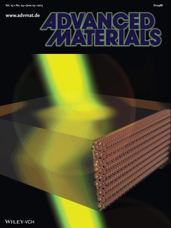
[25] W. Li, U. Guler, N. Kinsey, G. V. Naik, A. Boltasseva, J. Guan, V. M. Shalaev, and A. Kildishev, “Refractory Plasmonics with Titanium Nitride: Broadband Metamaterial Absorber,” Advanced Materials, vol. 26, no. 47, pp. 7959-7965, 2014. (Cover picture) [pdf]
[24] B. Saha, G. V. Naik, S. Saber, C. Akatay, E. A. Stach, V. M. Shalaev, A. Boltasseva and T. D. Sands, “TiN/(Al,Sc)N metal/dielectric superlattices and multilayers as hyperbolic metamaterials in the visible spectral range,” Physical Review B, vol. 90, no, 12, p. 125420, 2014. (Editor’s suggestion) [pdf]
[23] G. V. Naik, B. Saha, J. Liu, S. M. Saber, E. A. Stach, J. MK Irudayaraj, T. D. Sands, V. M. Shalaev, A. Boltasseva, “Epitaxial superlattices with titanium nitride as a plasmonic component for optical hyperbolic metamaterials,” Proceeding of National Academy of Sciences, vol. 2014. (Chosen for issue highlight) (Highlighted in Purdue News) [pdf]
[22] N. Kinsey, M. Ferrera, G. V. Naik, V. E. Babicheva, V. M. Shalaev, A. Boltasseva, “Experimental demonstration of titanium nitride plasmonic interconnects,” Optics Express, vol. 22, no. 10, pp. 12238-12247, 2014. [pdf]
[21] J. Liu, G. V. Naik, S. Ishii, C. DeVault, A. Boltasseva, V. M. Shalaev, E. Narimanov, “Optical absorption of hyperbolic metamaterial with stochastic surfaces,” Optics Express, vol. 22, no. 8, pp. 8893-8901, 2014. [pdf]
[20] J. Kim, G. V. Naik, A. V. Gavrilenko, K. Dondapati, V. I. Gavrilenko, S. M. Prokes, O. J. Glembocki, V. M. Shalaev, and A. Boltasseva, “Local Optical properties of gallium-doped zinc oxide—A low-loss plasmonic material: First-principles theory and experiment,” Physical Review X, vol. 3, no. 4, p. 041037, 2013. [pdf]
[19] U. Guler, J. C. Ndukaife, G. V. Naik, A. G. Agwu Nnanna, A. V. Kildishev, V. M. Shalaev, and A. Boltasseva, “Local heating with lithographically fabricated plasmonic titanium nitride nanoparticles,”Nano Letters, vol. 13, no. 12, pp. 6078-6083, 2013. [pdf]
[18] V. E. Babicheva, N. Kinsey, G. V. Naik, M. Ferrera, A. V. Lavrinenko, V. M. Shalaev, and A. Boltasseva, “Towards CMOS-compatible nanophotonics: Ultra-compact modulators using alternative plasmonic materials,” Optics Express, vol. 21, no. 22, pp. 27326-27337, 2013. (Top downloaded article since publication) [pdf]
[17] B. Saha, G. Naik, V. P. Drachev, A. Boltasseva, E. E. Marinero, and T. D. Sands, “Electronic and optical properties of ScN and (Sc,Mn)N thin films deposited by reactive DC-magnetron sputtering,” Journal of Applied Physics, vol. 114, no. 6, p. 063519, 2013. [pdf]
[16] T. R. Gordon, T. Paik, D. R. Klein, G. V. Naik, H. Caglayan, A. Boltasseva, and C. B. Murray, “Shape-Dependent plasmonic response and directed self-assembly in a new semiconductor building block, indium-doped cadmium oxide (ICO),” Nano Letters, vol. 13, no. 6, pp. 2857-2863, 2013. [pdf]
[15] G. V. Naik, V. M. Shalaev and A. Boltasseva, “Alternative plasmonic materials: beyond gold and silver,”Advanced Materials, vol. 25, no. 24, pp. 3264-3294, 2013. (Inside cover picture) [pdf]
[14] J. Kim, G. V. Naik, N. K. Emani, U. Guler and A. Boltasseva, ,”Plasmonic resonances in nanostructured transparent conducting oxide films,”IEEE J. Selected Topics in Quantum Electronics, vol. 19, no. 3, 2013. [Invited] (Cover picture) [pdf]
[13] M. A. Bodea, G. Sbarcea, G. V. Naik, A. Boltasseva, T. A. Klar and J. D. Pedarnig,”Negative permittivity of ZnO thin films prepared from aluminum and gallium doped ceramics via pulsed-laser deposition,”Applied Physics A: Materials Science & Processing, vol. 110, no. 4, pp. 929-934, 2012. [pdf]
[12] G. V. Naik, J. Liu, A. V. Kildishev, V. M. Shalaev and A. Boltasseva,”Demonstration of Al:ZnO as a plasmonic component for near-infrared metamaterials,” Proceedings of National Academy of Sciences, vol. 109, no. 23, pp. 8834-8838, 2012. (Highlighted in Purdue News) [pdf]
[11] G. V. Naik, J. L. Schroeder, X. Ni, A. V. Kildishev, T. D. Sands and A. Boltasseva, “Titanium nitride as a plasmonic material for visible and near-infrared wavelengths ,” Optical Material Express, vol. 2, no. 4, pp. 478-489, 2012. (Highlighted in OSA News release) (Top most downloaded article in two years 2011-2013) [pdf]
[10] U. Guler, G. V. Naik, A. Boltasseva, V. M. Shalaev, and A. V. Kildishev, “Performance analysis of nitride alternative plasmonic materials for localized surface plasmon applications,” Applied Physics B: Lasers and Optics, vol. 107, no. 2, pp. 285-291, 2012. [pdf]
[9] J. Kim, V. P. Drachev, Z. Jacob, G. V. Naik, A. Boltasseva, E. E. Narimanov, and V. M. Shalaev, “Improving the radiative decay rate for dye molecules with hyperbolic metamaterials,” Optics Express, vol. 20, no. 7, pp. 8100-8116, 2012. [pdf]
[8] M. Y. Shalaginov, G. V. Naik, S. Ishii, M. N. Slipchenko, A. Boltasseva, J. X. Cheng, A. N. Smolyaninov, E. Kochman and V. M. Shalaev, “Characterization of nanodiamonds for metamaterial applications,”Applied Physics B: Lasers and Optics, vol. 105, no. 2, pp. 191-195, 2011. [pdf]
[7] G. V. Naik, J. Kim and A. Boltasseva, “Oxides and nitrides as alternative plasmonic materials in the optical range,” Optical Material Express, vol. 1, no. 6, pp. 1090-1099, 2011. [Invited] (Top most downloaded article in two years 2011-13) [pdf]
[6] X. Ni, G. V. Naik, A. V. Kildishev, Y. Barnakov, A. Boltasseva, and V. M. Shalaev, “Effect of metallic and hyperbolic metamaterial surfaces on electric and magnetic dipole emission transitions Applied Physics B: Lasers and Optics, vol. 103, no. 3, pp. 553-558, 2011. [pdf]
[5] G. V. Naik and A. Boltasseva, “A comparative study of semiconductor-based plasmonic metamaterialsMetamaterials, vol. 5, no. 1, pp. 1-7, 2011. [Invited] [pdf]
[4] G. V. Naik and N. Bhat, Poly-ols based sol-gel synthesis of zinc oxide thin films, Journal of The Electrochemical Society, vol. 158, no. 2, pp. H85-H87, 2011. [pdf]
[3] P. R. West*, S. Ishii*, G. V. Naik*, N. K. Emani, V. M. Shalaev, and A. Boltasseva, Searching for better plasmonic materials, Laser & Photonics Reviews, vol. 4, no. 6, pp. 795-808, 2010. (Cover picture) (Highlighted by Purdue News) [pdf]
[2] G. V. Naik and A. Boltasseva, Semiconductors for plasmonics and metamaterials, physica status solidi (RRL) Rapid Research Letters, vol. 4, no. 10, pp. 295-297, 2010. (Focus issue on Nanoplasmonics) (in top 10 most downloaded paper in 2010-11) [pdf]
[1] Z. Jacob, J.-Y. Kim, G. V. Naik, A.& Boltasseva, E. Narimanov, and V. M. Shalaev, Engineering photonic density of states using metamaterials, Applied Physics B: Lasers and Optics, vol. 100, pp. 215-218, 2010. (Highest cited paper in APB during 2012) [pdf]
Patents
[5] V. M. Shalaev, A.V. Kildishev, G. V. Naik, A. Boltasseva, and U. Guler, “Titanium nitride plasmonic nanoparticles for clinical and therapeutic applications,” US application 20160120978 (2014).
[4] A. V. Kildishev, G. V. Naik, A. Boltasseva, U. Guler and D. Stocks, “Near- field transducer for heat-assisted magnetic recording,” US patent 9,343,088 (May 2016).
[3] G. V. Naik, B. Saha, T. D. Sands, V. M. Shalaev and A. Boltasseva, “Titanium nitride based metamaterial”, US patent application 20150285953 (Oct 2015).
[2] A. V. Kildishev, V. M. Shalaev, G. V. Naik, A. Boltasseva and U. Guler, “Refractory plasmonic metamaterial absorber and emitter for energy harvesting,” US patent application 20150288318 (2015).
[1] B.S. Amrutur and G. V. Naik, “Power Monitoring for Optimizing Operation of a Circuit” – US Patent 7,973,594 (2011).